Huawei's Pivot to a New Scaling Law
Sign up for ARPU: Stay informed with our newsletter.
Programming note: we will return next Tuesday with a look at SpaceX's IPO filing.
Folding the Factory
For decades, the chip race had one basic rule: make the transistor smaller.
That rule is Moore's Law—the principle, first observed by Intel co-founder Gordon Moore in 1965, that the number of transistors on a chip doubles roughly every two years, reliably delivering more computing power at lower cost. That relentless compression is what drives every device you own.
Moore's Law built Intel, TSMC, and the entire modern semiconductor supply chain. Shrink from seven nanometers to five, from five to three, from three to two—and the company with the best manufacturing process wins.
That is also how U.S. export controls were supposed to trap Huawei.
China cannot buy ASML's EUV lithography machines that make frontier chips possible. So the assumption was simple: without EUV, Huawei would stay several generations behind.
Then Huawei announced something strange this week.
At a semiconductor conference in Shanghai, the company's "Chip Queen," He Tingbo, announced that the future of chip scaling should no longer be guided by Moore's Law, but by a new principle they call the Tau (τ) Scaling Law.
When you cannot buy the tool that makes chips smaller, the next best option is to argue that smaller was never the whole point.
The Commute Problem
Shrinking the transistor is not an option for Huawei. But that constraint forced a question: is there a different lever to pull to make a chip faster?
To understand why their answer has genuine physical merit—and is not just a face-saving narrative—you have to look at something the industry has known for years. Making the transistor faster is only half the battle.
The industry currently relies on spatial scaling. You shrink the transistor (the "house") so you can fit more of them on a piece of silicon. But there is a catch. When you shrink the house, you also have to shrink the copper wire (the "highway") connecting it to the other houses.
When copper wires become microscopic, electrical resistance and parasitic capacitance skyrocket. In chip engineering, this is known as the RC Delay.
This creates an uncomfortable reality. The transistor does the math almost instantly, but the chip spends the rest of its time waiting for the data to fight its way through high-friction copper traffic. We are currently spending $300 million on a single EUV machine to build a faster transistor, only to trap its data in a microscopic traffic jam. It is like buying a Ferrari and exclusively driving it in a Manhattan tunnel.
Enter τ (Time). Huawei realized that signal propagation time—not transistor size—was a legitimate optimization target with real physics behind it. They stopped optimizing for space, and started optimizing strictly for time.
He Hui, director of semiconductor research at Omdia, described the shift to Reuters:
What Huawei is proposing is a shift from traditional node-driven scaling to system-level efficiency scaling. Rather than depending solely on smaller transistors, the company is focusing on shortening interconnect, lowering latency and improving data movement inside the chip, which is a credible way to extract more performance when leading-edge lithography is constrained.
Stacking the Factory
Huawei's answer is to fold the chip. Instead of spreading circuits flat across silicon, it stacks them vertically—turning the long horizontal commute into a short vertical trip.
That immediately raises a question: doesn't Nvidia already do something similar?
They do stack chips—but the stacking that exists today is mostly about memory, not logic.
Memory is just a filing cabinet. It stores 1s and 0s in a neat, predictable, repetitive grid. You can stack filing cabinets all day by simply drilling straight down through the layers.
Logic—the actual brain of the chip—is a factory floor. It is chaotic, hot, and full of crisscrossing wires routing data to different workstations. What TSMC and Nvidia do today is build a massive, flat logic factory, and park a skyscraper of memory right next to it.
Huawei cannot afford a massive flat factory. Stuck with bulky 7nm transistors, the floor would be too sprawling and the commute time for the data would kill the chip's performance.
So they did something much harder. Rather than stacking separately designed chips at the packaging stage, they distributed individual logic gates across multiple wafer layers during the design process itself. They chopped the logic factory in half and folded it on top of itself.
The math here is partly a long-term projection: Huawei claims that by 2031, this methodology will deliver transistor density equivalent to a 1.4-nanometer process. They are betting that folding their current nodes can eventually pack enough transistors to mimic the frontier. In the near term, Huawei claims an immediate 55% density increase and a 41% boost in power efficiency on their current chips. Zero ASML machines required.
The Skyscraper Catch
Of course, there is a very good reason the rest of the industry has not rushed into aggressive logic stacking. It is a thermal, manufacturing, and design-tool nightmare.
Logic circuits switch constantly, burn power, and create hotspots. In a flat chip, at least the heat has a reasonably direct path out. But when you start stacking active logic on top of active logic, some of the hottest parts of the chip are no longer sitting next to the heat sink. They are trapped inside the silicon high-rise.
That means the chip throttles, degrades, warps, or fails. The problem is not just heat; it is heat plus power delivery, mechanical stress, interconnect reliability, and manufacturing yield.
This is why the broader Huawei story is no longer just about chips. It is also about cooling, power, and data-center architecture. Huawei has been talking about tokens per watt, MW-level liquid cooling, and full-lifecycle thermal management. It is an acknowledgment that AI compute is becoming an energy-and-heat problem as much as a semiconductor problem.
But the harder constraint may be software. The global EDA ecosystem was built around mostly flat chips and increasingly sophisticated 2.5D packaging. True 3D logic is different. You cannot just take a 2D chip layout and click "rotate." The design software has to understand vertical placement, timing, heat maps, power delivery, signal integrity, and mechanical stress all at once.
So Huawei is not just trying to fold silicon. It has to build the design methodology for folded silicon. For this reason, the new approach is not merely a chip architecture. It is a bet that Huawei can rebuild enough of the surrounding toolchain—from circuit design to packaging to cooling—to make the architecture manufacturable.
The Forced Detour
In a nutshell, the U.S. export controls worked. They locked Huawei out of the spatial scaling track and gave TSMC and Nvidia a lead they can maintain for as long as ASML keeps shipping machines.
What Washington did not anticipate is what happens when you push a company this size to the edge of its options.
Nvidia CEO Jensen Huang told reporters this month that his company had "largely conceded" the Chinese AI chip market to Huawei. The sanctions were designed to keep China in the rear-view mirror. Instead, they pushed Huawei off the highway entirely—and onto a very hot new road.
Signal Stack
The operating reality beneath the headlines.
- Why Huawei Can't Catch Nvidia (Council on Foreign Relations) – Even doubling every aggressive production assumption, Huawei would still generate just 4% of Nvidia's aggregate computing power in 2026 — and its next chip will actually be less powerful than its best chip today.
- China Certifies 9 Domestic AI Chips for Government Procurement for the First Time (Tom's Hardware) – Beijing is systematically replacing Nvidia across state procurement, but all nine approved chipmakers are competing for slots at a single fab stuck at 7nm.
📊 Data > Narrative
We pull key data points to show you the mathematical reality of what's happening in tech.
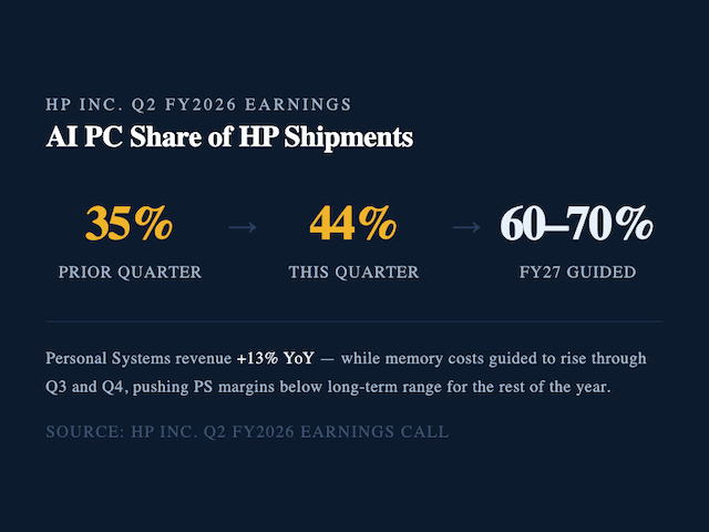
- The Data: HP's AI PC mix jumped from 35% to 44% of total shipments in a single quarter, with management guiding it to reach 60–70% in fiscal 2027. Personal Systems revenue grew 13% year-over-year. At the same time, memory and storage costs rose sequentially in Q2 and are expected to keep rising through Q3 and Q4, pushing Personal Systems operating margins below their long-term range for the rest of the year.
- The Takeaway: HP's earnings call is two stories running simultaneously. The first is that the AI PC transition is arriving faster than the market expected—nine points of mix shift in a single quarter is not a gentle trend, it is an inflection. The second is that it is arriving at exactly the moment when the components inside those PCs are getting more expensive. HP's management had to lock in memory supply for the full fiscal year through long-term agreements before the quarter even started.
You received this message because you are subscribed to ARPU newsletter. If a friend forwarded you this message, sign up here to get it in your inbox.