TSMC: Ending Semiconductor Cyclicality Through HPC
Sign up for ARPU: Stay informed with our newsletter.
In this week’s article, we will dissect the trajectory, capex and the end market shift of the world’s most dominant leading-edge chipmaker.
Founding History
Morris Chang’s path to founding the world’s largest pure-play foundry business was meandering and atypical.
When he was a young man, he dreamt of becoming a novelist. His father, a frequently relocating banker, however, didn’t think it was a good idea.
With the help of an uncle in Boston, he facilitated Chang’s admission to Harvard. The young undergraduate became instantly enamored with American culture, and the country’s economic and political might of the time. He decided to abandon his childhood dream and elected to become a mechanical engineer instead.
To further his employment prospects in the field, he transferred to MIT a year later. Eventually, he obtained his Master’s degree but failed to defend his PhD thesis on multiple occasions.
Following graduation, after a short stint at an electronics company, he moved to Texas Instruments to embark on a 25-year corporate climb. While at the company, an early experiment led him to a breakthrough in improving manufacturing yield (i.e. increasing the ratio of non-defective semiconductors relative to the entire output) by 20% and propelled him to a string of management jobs. TI also paid for Chang to complete his PhD in electrical engineering at Stanford.
While at TI, Chang came up with his first novel idea. He observed that every new semiconductor manufacturing run had the same problem. It was capital intensive and, during the initial phase, had to go through a learning period, when it was difficult to improve the manufacturing yield.
As a result, companies would simply charge high prices for the initial semiconductor product from the beginning to cover for the high costs of production and the low output.
Chang thought such an approach was flawed. So he engaged the Boston Consulting Group to devise a unique approach of using the learning curve to drive the pricing strategy, early in the life cycle of a new product.
TI and BCG were able to predict the unit costs in volume production on the basis of the actual cost of the first 1,000 units. They discovered that the cost per unit improved, as cumulative unit production increased over time.
So TI decided to sacrifice early profits and introduce a lower price for the initial product. This way the company was able to squeeze out competitors, gain market dominance and secure profitability down the line.
As Chang put it:
“We would automatically reduce, and then continually automatically reduce the price every quarter even when the market did not demand it. This was a very successful effort, even though it was somewhat controversial. A lot of people thought we were being foolish. Why would you reduce the price when you didn’t have to? But we did it because we believed in it, and indeed our market share just kept expanding. That, combined with other strategies, made the TI integrated circuits business the biggest IC business in the world, and also the most profitable.”
At the time, this idea was controversial, as companies would closely follow the cost curve (i.e. maximize profit with each level of output). However, now Chang’s strategy is a standard approach used across the industry.
He eventually left TI when he realized he was not going to enter the C-suite. Shortly after his departure, a government official in Taiwan approached him to head the Industrial Technology Research Institute, a government-sponsored non-profit with a mission to promote industrial and technological development in Taiwan. Even though his family and acquaintances advised him not to pursue this path, he decided to give it a shot.
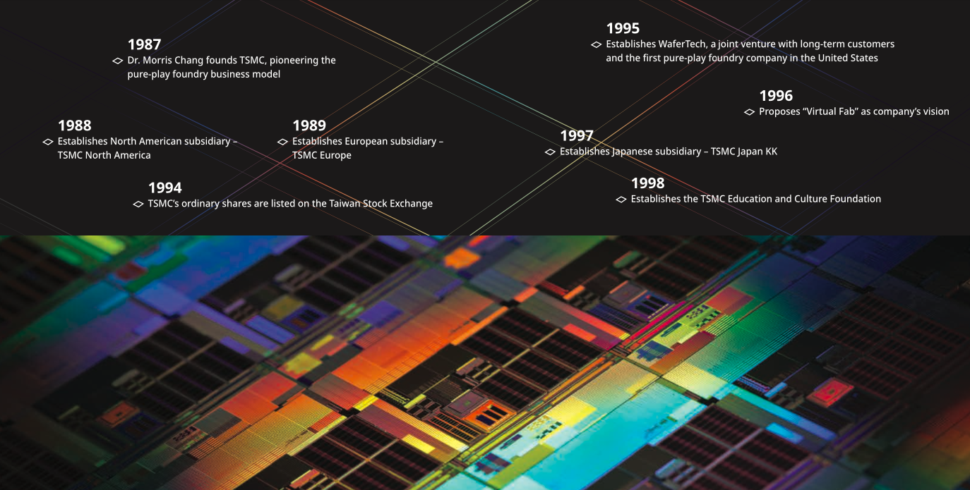
He started to shake things up at the Institute by putting low-performing employees on probation, and in 1987, at the specific request of the government he did not dare to refuse, Chang, then 56 years old, founded Taiwan Semiconductor Manufacturing Company, or TSMC, with $220 million in capital from Philips, the government of Taiwan, and private investors.
In the 80s, TI, Intel and AMD were strong players in the industry and Chang knew that Taiwan lacked the design and marketing prowess to go against them. So he decided to come up with an entirely new business category.
At the time, companies that designed chips but did not produce them (what we now call “fabless” companies) had a hard time with production. They were forced to accept very tough manufacturing deals from the likes of Fujitsu, IBM, TI or Toshiba.
These would often entail IP transfers or the prospect of the giants producing competing chips under their own labels. On top of that, they often had to wait for production until the dominant companies had extra capacity.
So Chang decided to found TSMC on a simple principle. The company would not design, manufacture or market any products under its own name and, instead, focus exclusively on manufacturing products for its customers. This way, TSMC would ensure that it never competes with its customers or makes its customers wait in a long line until capacity is freed up.
The company came to life right when companies started to see the value in outsourcing their manufacturing capabilities to Asia.
TSMC’s first customers included big companies like Intel and TI which were happy to outsource in-demand products that used outdated tech. Such an arrangement did not pose a big risk and allowed them to free their own capacity.
Soon, however, start-up companies that did not have the capital or the capacity to produce their own chips, such as NVIDIA, Qualcomm or Marvel came knocking at TSMC’s door.

Outsourcing to a company that was not a competitor was a saving grace for them. These companies could simply zero in on innovation and channel their funds into R&D without the need to transfer their IP for production. As Jen-Hsun Huang, NVIDIA’s founder put it, all of a sudden, TSMC reduced barriers to chipmaking, unlocking boundless creativity.
Through this approach, TSMC pioneered the pure-play foundry business model, enabled the rise of the global fabless industry, and quickly became one of the world's largest and most profitable chip makers.
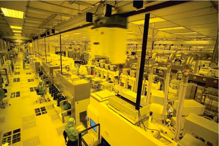
Headquartered in Hsinchu Science Park, Taiwan, TSMC currently serves 535 customers and uses 291 distinct technologies to ship well over 12,000 products a year.
The company is Taiwan’s biggest taxpayer and accounts for more than 7% of the country’s GDP.
In addition to its leadership in advanced process and specialty technologies, TSMC offers a comprehensive family of 3D silicon stacking and advanced packaging technologies.
It is known for long working hours, strict management, discipline and hierarchy. Over the past thirty years, TSMC has built up a complete ecosystem of suppliers around its production campuses and is able to mobilize engineers from multiple locations to enhance its operational efficiency.
In 2018, Chang retired with fame and fortune and was succeeded by C.C. Wei as CEO and Mark Liu as chairman.
Evolution
TSMC’s industry position is largely based on its technological leadership and manufacturing prowess. The company has been able to achieve both through massive capital expenditure and a relentless focus on enhancing its manufacturing capabilities.
As leading-edge microchips contain billions of transistors, and each new generation (referred to as a “node”) requires more transistors to be packed in to make them faster, more powerful, and energy efficient, the process technology for each new node also demands more complicated development and bigger investment in production capacity.
The amounts are not only massive (TSMC will spend $44 billion this year alone) but have to be spent on an ongoing basis for the company to stay at the leading edge.
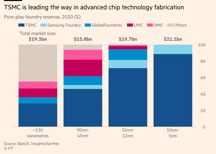
This is why TSMC grew so dominant. As the costs became higher, more chipmakers started to outsource their production, while competitors in the pure-play foundry such as GlobalFoundries gradually had to discard their ambition to compete with TSMC and drop out of the leading-edge race altogether.
Over the years, TSMC’s spending made the company a linchpin with the entire industry pretty much resting on its shoulders. Unlike 20 years ago, when there were 20 different fabs, most cutting-edge chips are now produced on a single campus in Taiwan.
TSMC currently controls a whopping 90% of the market for the most advanced nodes in production.
Such a position naturally gives it pricing power. TSMC has announced twice in less than a year that it will hike its prices to keep up with inflation and its massive expansion.
However, Capex is not the only issue. Shrinking transistors on microchips is also an engineering challenge. Intel, for example, has failed to master 10nm and 7nm technologies and had to outsource a portion of its manufacturing to TSMC.
Just to illustrate the point, a 3nm node has transistors with a size of just 1/20,000th of a human hair.
And to continue past the 5-nanometer process node, chipmakers need to use the extreme ultraviolet technology. ASML is the only company in the world that has mastered it. Their machines harness light that only naturally occurs in space to pattern the finest details on the most sophisticated chips. And TSMC channels a large portion of capital expenditure into buying this equipment.
As a result of supply chain disruptions, ASML’s capacity cannot keep up with demand. And because TSMC is in front of the line for placing orders, while ASML is constrained, potential competitors are kept at arm’s length.
In a way, both ASML and TSMC are monopolies. ASML owns EUV, while TSMC dominates leading-edge production. The marriage between the two currently makes both companies unassailable and also allows for the pursuit of Moore’s Law (i.e. doubling transistors every two years, while cutting costs in half) to continue.
TSMC is very focused on maintaining reliable production. At present, it operates four gigafabs whose combined capacity exceeds ten million 12-inch wafers.
Production within these facilities supports process technologies all the way to 5nm. 3nm is planned to start volume production in the second half of 2022, while R&D work on supporting the technology development of 2nm nodes and beyond is ongoing.
However, the shock from the auto chip shortage during the pandemic, the need to render advanced militarization less dependent on foreign manufacturing, and the mounting fear of the geopolitical whirlwinds surrounding Taiwan have led governments to believe that vital supply chains need to be brought closer to home.
As a result, TSMC has received a lot of political pressure from the US and Japan to spread their manufacturing outside Taiwan. The company committed to build a $12 billion 5nm plant in Arizona and to establish a subsidiary, Japan Advanced Semiconductor Manufacturing, Inc. (JASM), in Kumamoto, Japan, with Sony Semiconductor Solutions and DENSO to produce 12/16- and 22/28-nanometer technology.
However, this massive expansion has been plagued by a plethora of challenges. The tight US labour market coupled with Arizona’s hot climate meant that TSMC struggled to find adequate workforce for construction and had to accept delays in the timetable.
Given that it is relatively unknown in the US, the company also faces an uphill battle in securing scarce engineering talent. TSMC not only has to compete with better-known domestic behemoths such as Intel (which, unlike TSMC, is well-connected with American Universities, where engineering students are spoken for years before graduation) but also with the far more attractive tech highflyers. TSMC’s strict and hierarchical corporate culture, and lower salaries do not help in this battle.
Many have raised concerns that extending TSMC’s global footprint may hurt their margins (for example, production costs in the US are 8 to 10 per cent higher than in Taiwan) and undermine their efficiency, as clustering the same robust edifice of suppliers and engineers around their facility outside Taiwan is unlikely.
However, the cost gap of the $12 billion investment is subsidized by the US government and the hefty construction price tag is actually a drop in the bucket in comparison to the grand Capex scheme of things. The Arizona fab is also not as significant. By the time it comes online, it will already trail the 3nm facility in Taiwan.
So the expansion will not affect the business model much but it will also not significantly diversify production away from Taiwan.
Revenue Breakdown
As mentioned, TSMC is a dominant force in leading edge made-to-order chips.
In 2021, TSMC accounted for 26% of the worldwide semiconductor market, excluding memory and generated $56.82 billion in revenue (up 24.9 % from $45.51 billion in 2020) for a net income of $21.35 billion. Half of the revenue comes from advanced manufacturing processes (20% from 5nm and 30% from 7nm).
The story becomes really interesting when you look at the revenue breakdown by end markets.
In essence, TSMC serves five main markets, namely:
- Smartphone
- High performance computing, including PCs, tablets, game consoles, servers, base stations etc.
- Internet of Things, including various types of connected devices, such as smart wearables, health devices, home automation, surveillance systems, smart city etc.
- Automotive
- Digital Consumer Electronics, including digital TVs, set-top boxes, WLAN etc.
For each of these, TSMC has constructed five corresponding technology platforms to provide its customers with process and specialty technologies, IPs and packaging and testing technologies.
In the past, the smartphone segment was the company’s largest revenue generator. In 2021, smartphone unit shipments accounted for 44% of overall revenue and grew 6% relative to the prior year.
HPC came in second, accounting for 37% of overall revenue and grew at the rate of 10%. IoT was the fastest growing pocket, climbing at 30% and accounted for 8% of revenue. Cars and DCEs both contributed 4% with the latter being the only end market in decline, sliding 3% year-over-year.
However, when you look at the last quarter and listen closely to TSMC’s C-suite executives, it becomes evident that HPC is now the company’s primary growth engine. As smartphones slow down (growing sequentially at a meager 1%) and drop to 40% of revenue, HPC grows at 26% and becomes the largest contributor at 41% of revenue.
Here is the bullish proclamation from the CEO on the last earnings call:
“In fact, we expect our HPC platform to be TSMC's strongest growing platform in 2022 and the largest contributor to our growth, fueled by the structural megatrend driving increasing need for greater computation power and energy-efficient computing. But then more importantly, the increasing silicon content in end devices such as 5G smartphones, PCs, servers, networking and automotive applications are a much more important factor in supporting our strong semiconductor demand. And with our industry-leading technology, we are well positioned to capture all the opportunities.” – C.C. Wei, TSMC’s CEO, Q1 2022 Earning Call
The chipmaking giant’s geographical diversification is also strong. It calculates the division on the basis of the HQ of its customers. 64% of them come from North America, 15% from the Asia Pacific region, 11% from China, 5% from Europe, the Middle East and Africa and 5% from Japan.
The company is also highly profitable with an operating margin of 45.6% and an estimate of the long-term gross margin of 53% and higher.
The End of the Boom Bust Cycle?
The semiconductor industry is well-known for cyclical volatility, where huge investments lead to overcapacity that typically converges with softening demand.
Now, as Intel and TSMC plan their multiyear expansions worth hundreds of billions of dollars and demand in laptops, TVs and internet equipment is softening, some are ringing alarm bells.
However, as explained in this brilliant FT piece, a closer look at the HPC megatrend gives way to a different view.
In the past, chipmaking was powered by a few smart devices, such as smartphones and the end user was typically a consumer.
With the explosion of data and application innovation, however, things are shifting dramatically. The additional computation power required to store and process data gathered on devices and infrastructure means that the amount of silicon in each device is growing rapidly.
As an example, Applied Materials predicts that the chip content per datacentre server will rise from $1,620 to $5,600 in five years. And with this trend, the end market is shifting to large enterprises and governments which will likely impact the pricing structure.
As Martin Casado, a General Partner at Andreessen Horowitz recently put it, the boom in infrastructure and HPC is only getting started:
“We're still in relatively early innings for the cloud and there's a lot of workloads that should be in the cloud that are not, that are going to continue to move there […] I think we're just getting started. I literally think that like infrastructure is basically the beginning and the end of technology. Honestly, I believe that the future like vertical SaaS ends up becoming horizontal thin layers on top of core infrastructure components. And if infrastructure unlocks the capability of these apps to do new things, I just feel like we're in early innings of this. I think we've got decades of massive, massive growth. And I think a lot of the value is that most of the value will accrue to the infrastructure”.
TSMC’s CEO very much echoes this bullish sentiment. During the last earnings call, he said the following:
“On the demand side, despite the recent macro-related uncertainties, we continue to observe the structural increase in long-term semiconductor demand, underpinned by the industry's megatrend of 5G and HPC-related applications. This multiyear megatrend will support modest device unit volume growth, and much more importantly, drive substantial semiconductor content enrichment in many end devices across HPC, smartphone, automotive and IoT applications. With our technology leadership, TSMC is well positioned to capture the strong structural demand with our advanced and specialty technologies. And we expect our capacity to remain tight throughout 2022”.
Many experts, therefore, claim that the HPC explosion could put an end to the semiconductor industry’s past patterns of cyclical drops that occur every two to four years.
If you overlay two additional factors on top of it, namely that huge capital expenditure no longer leads to huge increases in capacity (10% to 15% at the most) and that customers build greater chip stockpiles to counteract weakening global supply chains, the typical boom bust cycle seems to no longer be a given.
What’s Next
In light of the increasing semiconductor content in most electronic devices, the early innings of the HPC explosion, the continued rise of fabless companies, the necessity of IDMs to outsource to TSMC, and TSMC’s unequivocal tech leadership in producing the most sophisticated chips, it is no wonder that the company expects its revenue to outpace the compound annual growth rate projected for the worldwide semiconductor market through 2026.However, the company’s production is highly concentrated in Taiwan. China’s threat of invasion and the increasing military and technological rivalry between the US and China render TSMC highly exposed to geopolitical turmoil.